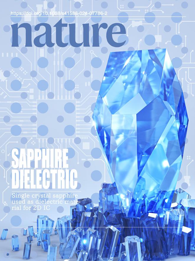
As the basic component of chips, the size of transistors is approaching the physical limit as chips shrink, and the gate dielectric material that plays an insulating role is very critical. The team led by Di Zengfeng, a researcher at the Shanghai Institute of Microsystem and Information Technology of the Chinese Academy of Sciences, has developed a single-crystal aluminum oxide gate dielectric material for two-dimensional integrated circuits - artificial sapphire. This material has excellent insulation properties and can effectively prevent current leakage even when the thickness is only 1 nanometer. The relevant results were published in the international academic journal Nature on August 7.

The results of the Shanghai Institute of Microsystem and Information Technology of the Chinese Academy of Sciences were published in Nature. The poster was provided by the interviewed team
"Two-dimensional integrated circuits are a new type of chip built with two-dimensional semiconductor materials with a thickness of only one or several atomic layers. They are expected to break through the physical limits of traditional chips. However, due to the lack of high-quality gate dielectric materials that match them, there is still a big gap between their actual performance and theory," said Di Zengfeng, a researcher at the Shanghai Institute of Microsystem and Information Technology, Chinese Academy of Sciences.
Di Zengfeng said that when the thickness of traditional gate dielectric materials is reduced to the nanometer level, the insulation performance will decrease, which will lead to current leakage, increase the energy consumption and heat generation of the chip. To deal with this problem, the team innovatively developed the in-situ intercalation oxidation technology.
"The core of in-situ intercalation oxidation technology lies in precisely controlling the orderly embedding of oxygen atoms into the lattice of metal elements layer by layer," said Tian Zi'ao, a researcher at the Shanghai Institute of Microsystem and Information Technology, Chinese Academy of Sciences. "Conventional alumina materials usually have a disordered structure, which leads to a significant decrease in their insulation properties at extremely thin layers."

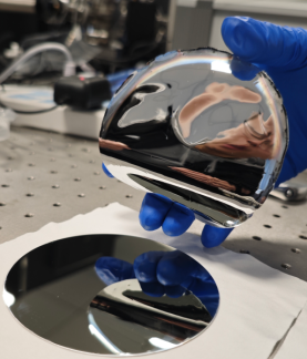
Aluminum oxide thin film wafer Photo provided by the interviewed team
Specifically, the team first used germanium-based graphene wafers as pre-deposition substrates to grow single-crystalline aluminum. Using the weak van der Waals force between graphene and single-crystalline aluminum, they achieved non-destructive peeling of 4-inch single-crystalline aluminum wafers. After peeling, the surface of the single-crystalline aluminum was atomically flat without defects. Subsequently, in an extremely low oxygen atmosphere, oxygen atoms were embedded layer by layer into the lattice of the single-crystalline aluminum surface, ultimately obtaining a stable aluminum oxide thin film wafer with accurate stoichiometric ratio and uniform atomic-level thickness.
Di Zengfeng introduced that the team successfully prepared a low-power transistor array using single-crystal aluminum oxide as the gate dielectric material, and the transistor array has good performance consistency. The breakdown field strength, gate leakage current, interface state density and other indicators of the transistor all meet the requirements of the international device and system roadmap for future low-power chips, and are expected to inspire the industry to develop a new generation of gate dielectric materials.
